Resources

Showing 11-14 of 14
  • Media Image
    Paolo Longo, Ph.D., Gatan, Inc. Sample courtesy of Professor Ramachandra Rao at Indian Institute of Technology, Chennai Madras, India Microscope courtesy of Dr. Giuseppe Nicotra at IMM-CNR, Catania, Italy

    Fe-O atoms are arranged in alternating tetrahedral and octahedral planes that can be distinguished looking at the fine structure of the O K-edge at 532 eV.

  • Media Image
    Paolo Longo, Ph.D., Gatan, Inc. Sample courtesy of Dr. Li Zhou at Ames Lab, Iowa

    EELS data taken using a FEI F20 TEM/STEM microscope equipped with S-FEG emission gun and a fully loaded GIF Quantum® ER system. Methods Voltage: 200 kV; data taken in STEM mode; EELS spectrum (300 – 2300 eV) exposure time: 8 ms; total exposure time:

  • Media Image

    The HAADF signal (left) contrast is easily interpreted in terms of mass thickness of the material while the diffraction contrast MAADF signal (right) reveals highly detailed structural changes in the material. The optimized geometry makes this possible.

  • Media Image
    This work was performed in collaboration with Dr. Phil Rice and Dr. Teya Topuria of IBM Almaden Research Center in San Jose, CA who provided expert assistance as well as the TEM specimen and access to their microscope facilities.

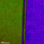
    Colorized EELS elemental map of Ti L2,3-edges at 456 eV (green), Mn L2,3-edges at 640 eV (blue), La M4,5-edges at 832 eV (purple) and Sr L2,3-edges at 1940 eV (red).

Pages