Resources

Showing 1-9 of 9
  • Methods

    As the size of III-V devices decreases, ohmic contacts and their performance becomes increasingly significant. . . .

  • Methods

    Over the past few years, with the advancements in aberration-corrected transmission electron microscopy, the spatial resolution in scanning transmission electron microscopy (STEM) has been enormously improved. . . .

  • Media Image
    Paolo Longo, Ph.D., Gatan, Inc.

    The EELS analysis shows how Pd particles chemically interact with support.

  • Media Image
    Paolo Longo, Ph.D., Gatan, Inc. Sample courtesy of Professor Ramachandra Rao at Indian Institute of Technology, Chennai Madras, India Microscope courtesy of Dr. Giuseppe Nicotra at IMM-CNR, Catania, Italy

    Fe-O atoms are arranged in alternating tetrahedral and octahedral planes that can be distinguished looking at the fine structure of the O K-edge at 532 eV.

  • Media Image
    Paolo Longo PhD, Gatan, Inc. Sample courtesy of Professor Robert Wallace at UTD, Richardson, TX Microscope courtesy of Professor Ray Carpenter, Arizona State University, Tempe AZ Acknowledgement to Dr. Toshiro Aoki at Jeol USA (now at ASU) for helping set up microscope for experiment.

    InP substrate is very beam sensitive; EELS analysis was carried out at high-speed to avoid electron beam-induced damage. Methods Probe-corrected Jeol ARM 200 TEM/STEM microscope; S-FEG emission gun; Enfinium™ ER system; voltage: 200 kV; STEM mode

  • Media Image
    Paolo Longo, Ph.D., Gatan, Inc. Sample courtesy of Professor David J. Smith at Arizona State University, Tempe, AZ Microscope courtesy of Professor Ray Carpenter at Arizona State University, Tempe, AZ Acknowledgement to Dr. Toshiro Aoki at Jeol USA (now at ASU) for helping set up microscope for experiment.

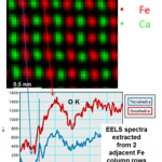
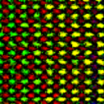
    Legend Red: Ti L at 456 eV; green: Sr L at 1940 eV; yellow: La M at 832 eV; blue: Mn L at 640 eV Methods Probe-corrected Jeol ARM 200 TEM/STEM microscope; S-FEG emission gun; Enfinium™ ER system; ​voltage: 200 kV; STEM mode; EELS low core-loss spectrum (280 – 2280 eV): 4 ms

  • Media Image
    Paolo Longo, Ph.D., Gatan, Inc. Sample courtesy of University of Glasgow Microscopecourtesy of Professor Gerald Kothleitner, TU-Graz, Austria

    Methods

  • Media Image
    Paolo Longo, Ph.D., Gatan, Inc. Sample courtesy of Dr. Giuseppe Nicotra at IMM-CNR, Catania, Italy Microscope courtesy of IMM-CNR, Catania, Italy

    Methods Probe-corrected ARM 200F TEM/STEM microscope; C-FEG emission gun; GIF Quantum® ER system; voltage: 60 kV; STEM mode; EELS low-loss spectrum (0 – 500 eV) exposure time: 0.01 ms; EELS core-loss spectrum (70 – 570 eV) exposure time: 10 ms; total exposure time:

  • Media Image
    Paolo Longo, Ph.D., Gatan, Inc. Sample courtesy of Professor Jianfang’s group, Chinese University, Hong Kong Microscope courtesy of IBM, Fishkill, NY

    Pd/Au alloys have attracted a lot of interest due to their resistance at high temperatures, and this explains their use in several fields, such as CO and hydrocarbon oxidation, synthesis of vinyl acetate monomer, hydrocarbon hydrogenation, and many others.