Locate Elements within Sample
Unique distributions of material at the nanoscale can create whole new classes of materials. Understand why EELS allows you to determine the spatial distribution of detected elements with near-atomic resolution in a modern TEM.
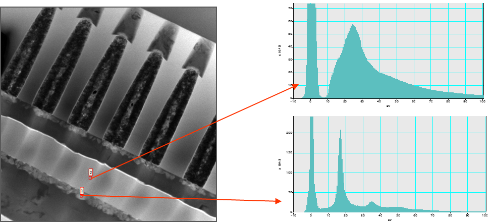
EELS is a high-resolution technique to better understand the spatial distribution of materials in your sample. This spatial distribution can be determined when you use a parallel beam on the sample to form an image (or series of images) with a narrow band of energies. This filtered imaging mode is known as energy-filtered transmission electron microscopy (EFTEM) and offers several operation modes that span the zero- and low-loss signals through the core-loss signals.
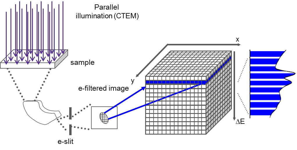
An alternative to acquiring a series of images is to create a spatially distributed collection of spectra or data cube. This method is known as spectral imaging (SI) or sometimes hyperspectral imaging. For EELS data, this spectral image can be constructed using a focused probe, collecting spectra pixel-by-pixel, or with a series of EFTEM images, collecting the cube energy plane-by-energy plane.
EFTEM
EFTEM provides methods of creating or enhancing image contrast to locate or quantify material in the sample. These methods include most probable loss imaging, contrast tuning, pre-carbon imaging, 3-window, jump-ratio (2-window), and chemical state mapping. Image quality with EFTEM is a function of the energy loss, energy-selecting slit width, and collection angle. The table below shows qualitatively the effect of the slit width and collection angle on EFTEM spatial resolution, while the following figure provides a more detailed description based on delocalization and optical aberrations. Even though delocalization and optical aberrations set the ultimate limit of the technique, it is more often the case that resolution is limited by the signal-to-noise ratio (SNR) of the image rather than optical aberrations. Parameters that increase the number of collected electrons have a strong impact on the SNR and, thus, on the actual image resolution.
| Resolution improves when | ||
|---|---|---|
| Factors affecting resolution | Slit width | Angle |
| Delocalization of inelastic scattering (Physics) | ||
| Chromatic aberration (Cc, width of slit) | ||
| Diffraction limit due to objective aperture | ||
| Spherical aberration due to objective lens (Cs) | ||
| Statistical noise due to small cross-sections | ||
| Signal-to-background | ||
| Radiation damage of the specimen | ||
| Instrumental instabilities (e.g., high voltage, sample) | ||
with being the characteristic scattering angle

3-window method for EFTEM mapping
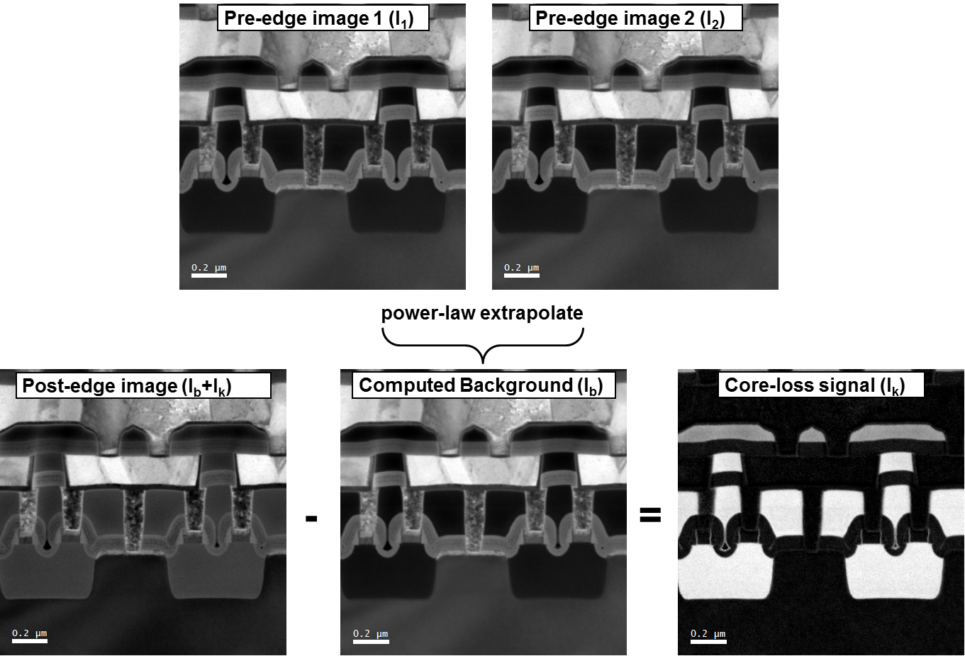
As diagrammed below, two pre-edge images are used to compute the background contribution to the post-edge image for each individual pixel in an EFTEM 3-window map. Subtraction of this computed background intensity from the post-edge image yields the core-loss signal.
To determine the net edge signal, simply compute and subtract the edge background using two pre-edge images as diagrammed below. With this method, a minimum of two background windows are needed. The map intensity is directly proportional to the projected concentration, and you can relate it to the absolute concentration if the thickness and elemental cross-sections are known.
Jump-ratio imaging
A jump-ratio image is formed by taking one image before (pre-edge) and one image after the edge (post-edge) so you can compute the ratio of the two. This provides a qualitative elemental image that directly relates to mass thickness of the element present. Jump-ratio imaging is useful in case of edge overlap, or difficult backgrounds at low energies. Jump-ratio mapping is particularly useful in cases where there is a small amount of a substance in a relatively uniform matrix (e.g., biological sections and polymer blends). This mapping also reduces diffraction contrast. However, be wary of artifacts when the thickness changes abruptly.

Visual representation of elemental mapping vs. jump-ratio imaging

Chemical mapping
Different chemical states of the same element often have characteristic spectral features that are sensitive to the types of chemical bonds present. Imaging with such features produces chemical maps (as opposed to elemental maps).

Spectrum imaging
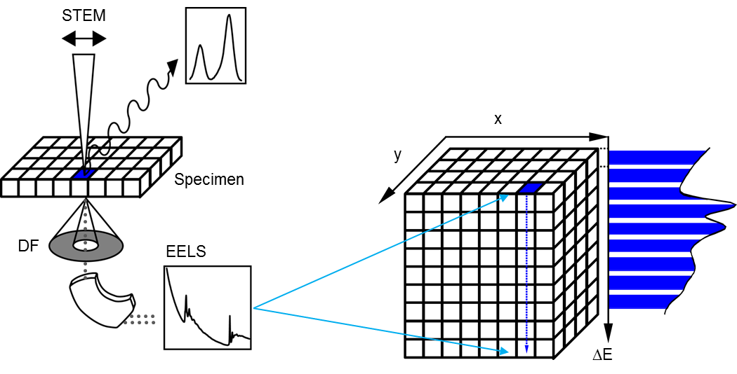
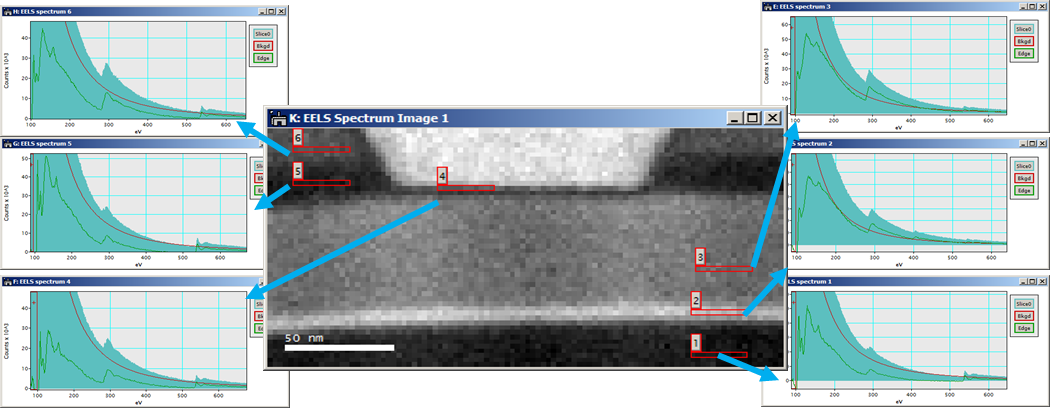
A spectrum image can be considered a data cube where each spatial point on one face of the cube projects down as an energy loss spectrum in the third dimension. Having a data cube has the advantage of allowing a full spectral analysis of each data point to be performed. This gives greater confidence in rejecting artifacts and allows processing decisions to be made and updated after the data has been acquired. The SI data cube can be acquired by scanning a focused probe over the sample in the scanning transmission electron microscope (STEM) to create a STEM SI; or use EFTEM to acquire images over a narrow band of energies to fill the spectrum image slice-by-slice to create an EFTEM SI.
STEM SI
Attain a STEM SI dataset by stepping a focused electron probe from one pixel to the next while you obtain a spectrum at each pixel. The spectrum image data cube is filled with one spectrum column at a time. STEM allows collecting any combination of signals (e.g., EELS, x-ray, and cathodoluminescence (CL) spectra) simultaneously. Acquiring the STEM image signal simultaneously permits spatial drift correction during acquisition.

EFTEM SI
When you utilize EFTEM to acquire a spectrum image (EFTEM SI), the energy filter is set to acquire an image that contains a narrow range of energies. The spectrum image data cube is filled with one energy plane at a time.
EFTEM SI examples of typical energy resolution
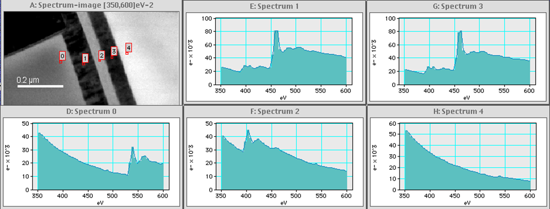
EFTEM SI samples at high (<1 eV) energy resolution
