Getting Started

Learn about the important parameters you will need to optimize each EELS experiment, including sample preparation, electron microscope setup, technique selection, and collection angle considerations. Understanding the effect of these key parameters will help ensure a successful EELS experiment and improve the quality of your analysis.
Sample Requirements
Like all experiments in the TEM, data quality is only as good as the sample put in the TEM. In general, samples should be thinned to electron transparency using a method that does not introduce artifacts. The sample needs to be electrically conductive and rigidly supported by the sample holder. Surface damage layers should be minimized. For STEM experiments in particular, any contamination of the sample, its holder or the TEM vacuum by hydrocarbons, silicone oils or similar chemicals will lead to rapid sample contamination under the beam and must be avoided.
Select appropriate sample thickness
A successful EELS experiment begins with a clean, electron-transparent sample. Depending on the data required, the sample needs to be between 0 – 6 times the local mean-free path (mfp). For 200 kV electron, the mfp of most materials is on the order of 80 – 120 nm; however, it has a strong variation with Z, density, and the TEM accelerating voltage.
The sample geometry can also affect the optimal sample thickness simply due to sampling considerations. Consider the case of precipitates in a wedge-shaped sample. For thick regions, the precipitates will be abundant, but they represent a small fraction of the volume the beam interacts with. In addition, the EELS data may have high background due to multiple scattering in thick regions. In very thin regions, there may be no precipitates to measure. Grain boundaries and interfaces pose similar constraints.
Below are sample thickness guidelines that correlate to the type of EELS analysis you may want to perform.
|
Application |
Sample thickness (mfp) |
|---|---|
|
Qualitative mapping (edges <800 eV) |
0.1 – 1.2 |
|
Qualitative mapping (edges >800 eV) |
0.3 – 2.5 |
|
Quantification |
0.1 – 1.0 |
|
Quantification (edges >1.5 keV) |
<1.5 – 2.0 |
|
Energy loss near edge structure (ELNES) mapping |
~0.0 – 1.5 |
|
Thickness maps |
<6.0 |
|
Plasmon energy analysis |
0.1 – 6.0 |
|
Low-loss EELS analysis |
0.1 – 3.0 |
|
Low-loss EELS analysis with deconvolution |
0.5 – 6.0 |
Sample's contribution to image drift
Common environmental factors, including vibration, thermal variations, and stray electromagnetic fields, can cause your sample to drift during an experiment. This drift may cause image blurring that impacts the resolution and quality of your data. Below are frequently encountered sources of drift related to the sample itself:
-
Charging
-
Symptoms – Sample drift or jumping will increase as more beam is applied or when the objective aperture is inserted or removed from the system
-
Solution – Coat your sample with carbon to make the sample conductive
-
-
Improper sample mounting
-
Symptoms – Sample vibrates or appears loose on the grid or in the holder
-
Solution – Verify how securely fastened the sample is to the grid or holder
-
-
Beam sensitivity
-
Symptom – Sample appears to be shrinking
-
Solutions
-
Coat your sample with carbon to make the sample conductive
-
Condition (controllably stabilize) the sample with a large area, low-intensity beam prior to starting your experiment
-
Reduce the electron dose
-
-
References
Malis, T.; Cheng, S. C.; Egerton, R. F. “EELS log ratio technique for specimen-thickness measurement in the TEM” J. Electron Microscope Technique 8 (1988) 193
TEM Setup for Analysis
Before you start an experiment, the TEM must be well aligned. The emitter, condenser, and optic axis adjustments typical for your TEM type should be performed. This will help maximize image brightness and minimize lens aberrations.
-
Insert your sample into the column (if possible, first plasma clean the sample).
-
Find the region of interest you want to investigate.

-
Align the TEM; critical for energy-filtered TEM (EFTEM).
-
Set TEM to eucentric focus value and bring the sample to the eucentric height.
-
Check the condenser alignment.
-
Align the optic axis (use HT-centering if available; alternatively, rotation center or coma-free centering can be used).
-
Clear the beam path to the filter (retract unused detectors and raise the viewing screen).
-
-
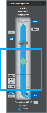
From the user interface on your TEM, enter the Gatan imaging filter (GIF) or EFTEM lens series (if available) for your TEM.
Note: The GIF or EFTEM lens series serves two critical functions.-
Stabilizes the position of the projector crossover so the EELS spectrum will stay in focus at the slit for all TEM magnifications.
-
It lowers the apparent magnification of the TEM to compensate for the increased magnification of the GIF, allowing a larger field of view and easier control of the TEM stage and adjustments.
-
-

Select Unfiltered.
Prepare the GIF for imaging.
Note: It is often helpful to locate the GIF field relative to the screen center for viewing. Identify a prominent feature in the sample on the GIF camera, then lower the viewing screen. Make a note of the position of the feature relative to the screen center.-
From the Microscope System palette in the DigitalMicrograph® 3 software.
-
Select the EFTEM control button to place the GIF in image mode.
-
Right-click the EFTEM control button to select Unfiltered from the Regime dropdown list.
-
-
Double-click the GIF camera icon within the Microscope System palette to start the camera view, or select View from the Camera palette in the Techniques Manager.

Select View.
-
You should now have an image of the specimen on the view screen. If no image appears,
-
Ensure the screen is lifted, and no other detectors are in the beam path.
-
With the screen down, check that the central area of the screen is illuminated.
-
-
-
-
Preview filtered image.
-
Choose Zero-Loss regime from the drop-down list or check the Insert Slit box.

Choose Zero-Loss regime.

Or check the Insert Slit box.

-
If necessary, run the Center ZLP command to center zero-loss peak within the slit.
-
-
Take a thickness (\(t/\lambda\)) map.

- Under the EFTEM technique, choose the \(t/\lambda\) button.
- If the buttons are not visible, make sure SingleMap mode is selected in the EFTEM pallet.
- As a default, choose Auto checkboxes for the Exposure and CCD binning settings.
- Choose OK to acquire the map.
 Evaluate the sample's local thickness (in mfp) from the thickness map and compare itto the typical required values above.
- Under the EFTEM technique, choose the \(t/\lambda\) button.
Technique Selection
During the planning phase of each experiment, it is important to know what questions you want to answer, including what elements you are looking for, how much, their location, and the chemical state. When combined with information you already know, such as your sample's geometry or some major and minor elements, it is easier to select an appropriate technique that delivers answers in the shortest time possible.
-
Individual spectra from a few well-chosen points – Typically gives the highest quality spectra and quantification; you can acquire data in STEM or TEM mode.
-
Electron spectroscopic imaging (ESI) or contrast tuning – Powerful technique used to image one energy loss window (e.g., zero–, plasmon– or pre-carbon loss) or to scan for different phases or defects
-
Defects and changes in material properties often show strong contrast at specific energies.
-
-
Jump-ratio imaging (2-window mapping) – Allows mapping of elements via the ratio between post-edge and pre-edge energy-filtered transmission electron microscopy (EFTEM) images; works best for finding small amounts of one element in an otherwise uniform matrix.
-
Elemental mapping (3-window mapping) – Allows mapping of elements using two pre-edge EFTEM images to estimate the background under a third post-edge EFTEM image; works best for mapping elements in a general sample type.
-
STEM and EFTEM spectrum imaging (N-window mapping) – Mapping and analysis via collection of a complete spectrum at each point of an image; allows superior background subtraction for standard mapping and allows advanced analysis techniques
References
Egerton, R.F. Electron Energy Loss Spectroscopy in the Electron Microscope. Springer. 3rd ed. New York: 2011.
Collection Angle Considerations
To optimize the collection efficiency and spatial resolution of the EELS signal, it is a prerequisite to understand how electron scattering and collection angles can impact your signal.
Characteristic scattering angles
The scattering process must conserve both energy and momentum. The momentum change perpendicular to the beam is seen as a change in the angle of the electron. Parallel momentum change does not deflect the electrons. The inelastic scattering distribution will have a Lorentzian distribution with a characteristic angle, \(\Theta _{E}\), given by the approximate relation for high energy electrons:
\(\Theta _{E}=\frac{E_{edge}}{2E_{0}}\)
where
-
\(E_{edge}\) = Edge energy
-
\(E_{0}\) = Primary beam energy
The EELS signal is highly forward scattered, but for higher energy edges, the distribution can become broad. In addition, the Lorentzian distribution has significant tails; it is recommended that the EELS collection angle be set to 3x \(\Theta_{E}\) to optimize the ratio of signal to background. Larger angles continue to increase the background contribution but have little effect on the edge signal. Note that this recommendation assumes a mostly parallel incident beam and no strong elastic scattering. Larger angles are often necessary when aligned to a zone axis due to the strong elastic scattering to high angles, and for Cs corrected STEM when the convergence angle is often larger than the recommended 3x \(\Theta_{E}\) above. However, the graph below is a useful baseline to help optimize the collection angle for your individual sample.

|
\(E_{0} = 200 keV\) |
Si L |
C K |
O K |
Cu L |
Si K |
Au M |
Ti K |
|---|---|---|---|---|---|---|---|
|
\(\Delta E (eV)\geq\) |
99 |
284 |
532 |
931 |
1839 |
2206 |
4966 |
|
\(\Theta E (mrad)\) |
0.29 |
0.83 |
1.55 |
2.7 |
5.3 |
6.4 |
14.4 |
|
\(2\Theta E (mrad)\) |
0.58 |
1.65 |
3.0 |
5.4 |
10.7 |
12.8 |
28 |
|
\(3\Theta E (mrad)\) |
0.86 |
2.4 |
4.6 |
8.1 |
16.0 |
19.2 |
43 |
Measure the collection angle
Once you identify the appropriate collection angle, you will need to apply this setting on your electron microscope. Below are graphics that outline how to determine the collection angle based on the technique you select.
STEM and Diffraction mode

EFTEM – Imaging mode

References
Egerton, R.F. Electron Energy Loss Spectroscopy in the Electron Microscope. Springer. 3rd ed. New York: 2011.